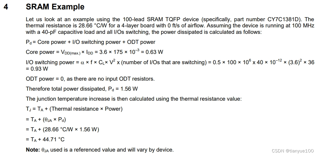
Understanding Thermal Resistance in the Real World
Introduction There can be significant differences between the thermal characteristics stated on a device’s datasheet and what actually happens in a real world application. Semiconductor manufacturers usually provide thermal resistance values for Junction to Case (RθJC) and Junction to Ambient (RθJC). Although these are extremely useful parameters to estimate a device power handling capability, there can still be a disconnection between those figures and reality.
This note will illustrate how the thermal data provided in manufacturer’s datasheets compare to real world applications and will also discuss the relative thermal performance of Diodes Incorporated’s PowerDI® 5060 package against similar competitor packages.
Thermal Resistance and MOSFET packages
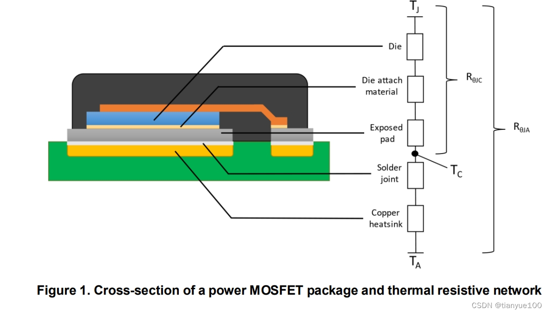
Junction to Case thermal resistance is a MOSFET's intrinsic characteristic that refers to the thermal resistance inside the device package. RθJC is a fixed value defined by die size and package design. This means that RθJC deals with the power dissipated in the device only. For the purpose of this application note RθJC refers to the thermal resistance from the junction to the bottom of the exposed pad. On the other hand, Junction to Ambient thermal resistance is made up of all thermal resistance involved in the heat flow path from the die to the outside environment and it is much more dependent on the board's layout and heat sinking capability. For example, if we modify the size of copper area where heat is dissipated RθJC is expected to change. The figure below gives a visual representation of the thermal resistive network inside a MOSFET.
As most of the heat generated by the MOSFET will be dissipated through the copper heatsink on the PCB, it follows that the larger the heatsink area is the lower RθJC will be. Conversely, the opposite happens if the area is reduced. Thus, RθJC is the dominant thermal resistance in an application.
To understand the influence of RθJA in a device, the thermal behavior of MOSFETs in the DMTH family were tested in 5 different packages:
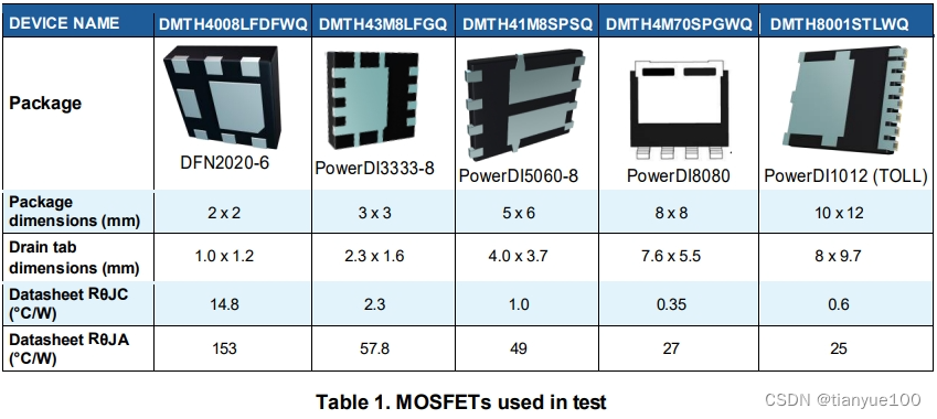
All devices were mounted on multiple 1oz copper, single-layer, FR-4 substrate boards with no additional heatsink attached. The drain pad area in each board ranged from the minimum allowed by package to a 25.4 × 25.4mm (1-inch) copper pad.
Thermal characterization was performed with a dedicated thermal analyzer to find the temperature coefficient and consequently the Junction to Ambient thermal resistance of each board. A graph of thermal resistance in function of drain pad area was plotted with the collected data.
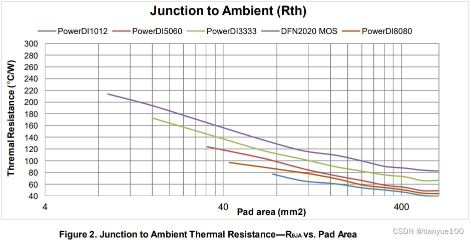
We can see from Figure 2 a continuous decrease in thermal resistance as the copper area gets larger. The lowest RθJA is achieved with the largest copper area regardless of the package. Note that RθJA values scale up as the package gets smaller though a fairly constant difference is kept between the five datasets all along. Since all devices are tested under the same conditions this difference can only be due to package size and the die itself, in other words its RθJC.

It can be seen that PowerDI® 1012 exhibits the best power dissipation capability of all five packages reaching 2.62W on the largest drain pad. Due to its size, the device can hold greater currents allowing for more power dissipation. Likewise, heat will spread more effectively over its larger area in comparison with other packages.
For the PowerDI® 8080 and PowerDI® 5060 there is a fairly constant difference of 0.2W.
In the case of DFN2020 and PowerDI® 3333, the power dissipation difference on a drain pad of up to 70mm² is less than 100mW growing to a maximum of 360mW at the largest area.
Power dissipation for each device can be calculated with the following formula:
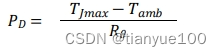
Where 𝑇𝐽𝑚𝑎𝑥 is the maximum temperature rating of the junction inside the die, 𝑇𝑎𝑚𝑏 is assumed to remain constant at 25°C and 𝑅𝜃 in this case is RθJA. The power dissipation of the 5 MOSFETs was calculated obtaining the following results:
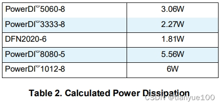
These results appear to be close to datasheet figures. However, it is important to remember that these come from a theoretical calculation. Figure 3 shows that the actual power dissipation is lower than the calculated value. The main reason being the different conditions and environment in which thermal testing was performed.
Thermal management techniques are normally used to greatly reduce the thermal resistance of a PCB and its components. The addition of GND planes, thermal vias and extra copper reduces the RθJA and so allows for greater power dissipation. It is the case with PowerDI®5060 that although the same RθJA value of the datasheet was obtained in test, the power dissipation shown in datasheet is about 1W above the measured value.
Comparison under same conditions of PowerDI® 5060 and competitor
To have a better understanding of how thermal characteristics affect real-world performance we compared DIODES DMTH41M8SPSQ* N- channel MOSFET with a competitor component of similar characteristics. Both devices use copper clip bonding rather than bond wires to common drain and come in a same-size package.
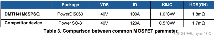
The RθJC of DMTH41M8SPSQ is 1.0°C/W while the competitor's part claims a RθJC of 0.5°C/W on its datasheet and does not provide a RθJA value. The omission of this parameter in the datasheet leads the designer to make the common mistake of using RθJC when calculating power dissipation. Recalling Figure 1, we saw that RθJA is already comprised of RθJC so the correct value to use in calculation is RθJA. The graph below shows the actual RθJA of both devices under the same conditions.


Where the power dissipation difference is minimal just as with thermal resistance in Figure 4. Another test was performed with appropriate equipment to measure the actual power dissipation.

The graph above shows that the resulting power dissipation lines overlap making the difference barely noticeable. This only confirms that the performance of both devices is nearly the same.
So far, both graphical and numerical results tell that neither device can be considered 'thermally superior' but then, what is the difference between these two?
A second test was performed, this time to compare the RθJC of both MOSFET’s. The devices were mounted on a piece of a solid copper plate that approximates an infinite heatsink and the same amount of power was dissipated through them. The devices were kept at a constant ambient temperature with a computerized thermostat, this way the only thermal resistance obtained was between the die and soldering point.
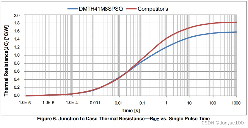
The graph above shows RθJC recorded for various single pulses, where at steady state DMTH41M8SPSQ has an RθJC value of 1.57°C/W while competitor's device 1.81°C/W. The behavior of both devices is similar for pulses of less than 30ms. Although the graph confirms that there is an RθJC difference of 0.24°C/W, it turns out to be half of what can be calculated with datasheet values.
In a real application, most of the heat power is going to be dissipated through the PCB where the dominant Thermal Resistance is RθJC because of its larger magnitude compared to RθJC In our comparison, both devices showed a similar behavior in Thermal Performance and almost identical results in Power Dissipation ensuring that a small difference in RθJC has little to no impact in actual applications.
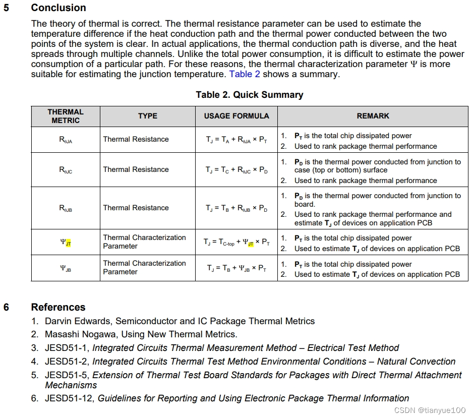
Conclusion
It is true that datasheet values give precise information about a device, but when it comes to thermal information this has to be treated as reference only and may not reflect the real thermal behaviour of a device. Ambient conditions vary depending on the application and apart from thermal resistance values found in datasheets; package size and board design also play an important role in thermal resistance and consequently in power dissipation. Not only that, various techniques can also be used to manage heat dissipation on a board and its components.
In most applications RθJA is dominated by PCB effects while RθJC is just a small part of the overall system. Although RθJC easily provides a consistent measure on a device level it does not reflect the key aspect of and actual application which is the device thermal performance at a system level.
In the case of devices with same-sized packages, performance resulted slightly different from what could be assumed by only reading the datasheet. In our comparison, the thermal behavior and power dissipation capability of two physically similar devices from different manufacturers was proved to be the same. This would be true for any other 5 x 6 packages if they were put under similar conditions. Thus, their small difference in RθJC does not necessarily mean better or worse performance in the real world.
It its worth reminding that as complex as it is, thermal information is based on empirical results that were measured under specific test conditions and must be used as a design aid and not as absolute values.
*Q - Automotive-compliant - AEC qualified, manufactured in IATF 16949 certified sites supporting PPAP document
Understanding Semiconductor Thermal Resistance Data
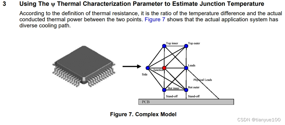
Understanding Semiconductor Thermal Resistance Data (diodes.com)![]() https://www.diodes.com/assets/Articles/Steady-State-Thermal-Values.pdfSemiconductor devices are not perfect ‐ all diodes and transistors are characterized by power losses due to switching and conduction. Switching losses occur during the interval between the on‐ and off‐states of a junction, when there is both a voltage across the device terminals and a current flowing through it. Conduction losses are due to the device’s internal resistance that, no matter how low it is, will result in a power loss when a current is flowing. Even in the off‐state, losses due to transistor leakage currents can be significant in devices such as microprocessors that have to use small geometry processes in order to pack millions of transistors into a single integrated circuit.
https://www.diodes.com/assets/Articles/Steady-State-Thermal-Values.pdfSemiconductor devices are not perfect ‐ all diodes and transistors are characterized by power losses due to switching and conduction. Switching losses occur during the interval between the on‐ and off‐states of a junction, when there is both a voltage across the device terminals and a current flowing through it. Conduction losses are due to the device’s internal resistance that, no matter how low it is, will result in a power loss when a current is flowing. Even in the off‐state, losses due to transistor leakage currents can be significant in devices such as microprocessors that have to use small geometry processes in order to pack millions of transistors into a single integrated circuit.
Whatever the cause, losses in semiconductor devices generate heat that has to be dissipated if the junction temperature is to be kept within acceptable limits for correct device operation. The packaging of semiconductor devices further complicates the means by which heat can be dissipated so it is important to understand the various processes involved and the way in which thermal information is provided in device datasheets.
This article will look at the mechanisms by which heat is normally dissipated, aiming to understand in what way these apply to semiconductor devices and in turn how the semiconductor manufacturers specify the thermal performance of their products. The inaccuracies that can arise from using the thermal information provided in the datasheet will be highlighted along with an alternate method of determining the key junction temperature of a device.
Mechanisms for Heat Dissipation
There are three basic mechanisms by which heat is dissipated from an electronic device: conduction, convection and radiation. For a packaged semiconductor device the majority of the heat will be transferred by conduction: from the heat source at the device’s core through the semiconductor substrate, the lead frame to which the chip is attached, and through the molding material that encapsulates the device to its external surface. At this point heat may be further transferred by conduction through any solid material the device is in contact with, e.g. a printed circuit board or an external heatsink.
Convection is defined as the transfer of heat via a fluid, which may be a liquid or gas, as in the surrounding air. This is the mechanism that then largely accounts for the remaining heat dissipation to the surrounding ambient environment. Radiant heat transfer is rarely a significant mechanism for heat transfer in electronics and is complex to calculate because it not only depends on temperature difference but also by the distance between objects and factors such as the color and texture of surfaces.
Although effective heat transfer from source to ambient is the aim, it is more usual to determine heat dissipation by considering the inverse of heat flow, namely the thermal resistance between those points. Typically this figure will be made up from the thermal resistances between the end‐points and one or more intermediate points, depending on the heat transfer mechanisms and the materials involved.
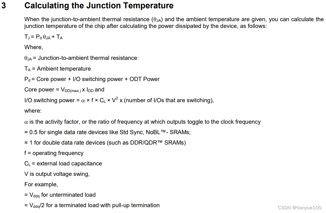
Semiconductor manufacturers provide thermal resistance values for packaged devices as a design aid to help determine their power handling capability. Normally given as a junction‐to‐ambient thermal resistance, this figure is intended to allow calculation of the amount of power that can be safely dissipated inside a device without raising its junction temperature (Tj) above its specified maximum. For example, for a device operating in an ambient temperature (Ta) of 25°C that has a junction‐to‐ambient thermal resistance, Rth (JA), of 150°C /W with a specified maximum junction temperature, Tj, of 150°C, the maximum power (Pmax) can be calculated using the following formula:
Pmax = (Tj (max) – Ta)/Rth (JA) = (150‐25)/150 = 0.83W
Note: This assumes the device is mounted under the same conditions for which Rth(JA) is defined in the datasheet.
Conversely from this formula, Tj can be calculated by knowing the power being dissipated inside the device and the Rth (JA) and Ta values.
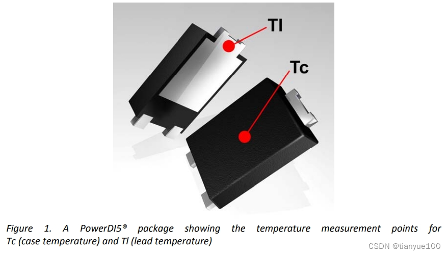
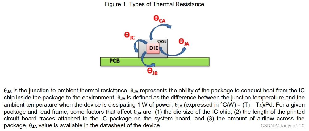
Sometimes manufacturers will provide alternative or additional thermal resistance values, which can be used in a similar way to calculate the operating junction temperature. These might include the junction‐to‐case (top of the package) value, Rth (JC), and the junction‐to‐lead value (junction to the soldering point of the lead frame), Rth(JL) – see figure 1.
Trying to measure the thermal resistance of a specific heat flow path like junction‐to‐case or junction‐to‐lead is complicated by the fact that the power dissipated at the semiconductor junction leaves the package through a number of parallel heat flow paths. Each of these has a specific thermal resistance whose value depends on the dimensions and the thermal conductivity of that path. Consequently a meaningful thermal resistance figure depends on 1) how accurately temperatures at the junction and case (or lead) can be measured and also 2) determining the fraction of the total heat generated at the semiconductor junction that is flowing between the junction and the measurement point (i.e., either the top of the case or the lead).
In practice, obtaining accurate temperatures at the required measurement points is difficult, even using non‐contact infrared instruments. Instead, one of the following JEDEC (JESD51‐12) standard methods may be used to determine thermal resistance values for Rth (JC) or Rth (JL).
Method 1: Rth(JX_Ө)
This method aims to determine the thermal resistance of a heat flow path between the junction and a specific point of interest, ‘X’, which could be the top of the package, a soldering point, etc. Method 1 assumes that all the power dissipated at the junction is forced through the point of interest using an effective heat sinking arrangement at point ‘X’. Then with an accurate measurement of temperature at that point (Tx) the true thermal resistance can be calculated as:
Rth(JX_Ө) = (Tj –Tx) / P
Where P is the dissipated power (heat) that flows from the junction to the point ‘X’. Ideally, during this measurement, close to 100% of the power should flow from the junction to the point ‘X’. This figure depends only on the physical properties of the heat flow path and is independent of the amount of power dissipated or the size of board the device is mounted on.
The junction‐to‐lead thermal resistance values provided by Diodes Incorporated in its datasheets are measured using Method 1. The value is independent of board size and so helps compare the thermal performance of the lead frames of various packages.
Method 2: Rth(JX_ᴪ)
This method provides a thermal characterization parameter, which should not to be confused with thermal resistance. It is calculated using an equation similar to that used in method 1:
Rth(JX_ᴪ) = (Tj –Tx) / P
With this method, because no additional heat sinking arrangement is used to divert most of the generated heat through the path of interest, the total dissipated power value is used in the calculation instead of the fraction that is flowing between Junction and point ‘X’. This results in a lower absolute value for Rth(JX_ᴪ).
The junction‐to‐case thermal resistance values provided by Diodes Incorporated in its datasheets are measured using Method 2, which is why subsequently in this article Rth(JC) will, more correctly, be referred to as ᴪth(JC).
Determining the junction temperature (Tj):
Accurately determining the junction temperature (Tj) of a device using Rth(JA), Rth(JL) or ᴪth(JC) depends on being able to measure ambient, lead or case temperatures under ideal datasheet conditions. In reality, a device will often be mounted on a circuit board crowded with other devices and components; also the amount of copper connected to the lead frame tab may not match the datasheet’s conditions, limiting the usefulness of these parameters as discussed below:
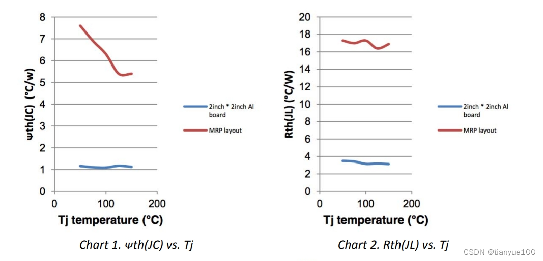
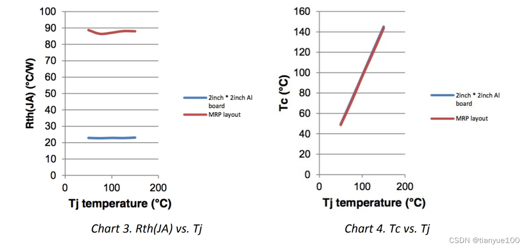
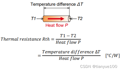
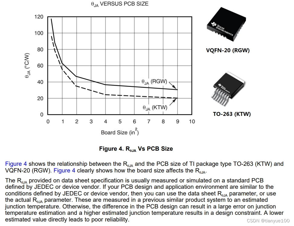
Charts 1 to 3, measured on a PowerDI package (as shown in figure 1), show the relationship between junction temperature and ᴪth(JC), Rth(JL) and Rth(JA) respectively, under the different heatsink conditions of: 1) a 2inch * 2 inch aluminum board and 2) a Minimum Recommended Pad (MRP) layout.
Rth(JA) … As shown in Chart 3 the variation of Rth(JA) with junction temperature is minimal but the impact due to different heatsinks is more significant. Consequently when using datasheet Rth(JA) values care must be taken to make sure that device mounting conditions in actual applications are close to those stated in the datasheet. The differences in heatsink arrangements (volume and conductivity of the heatsink connected to the lead frame tab of the device) can cause significant errors when estimating the junction temperature using Rth(JA).
Rth(JL) … This value is measured according to JEDEC (JESD51‐12) Method 1 and can only be used 1) if the heat flow in every other path is made insignificant and 2) the lead temperature is measured accurately. In order to measure the datasheet Rth(JL) value using this method, it is necessary to attach a massive heatsink to the lead frame tab to ensure that most of the heat from the junction flows out of the lead frame tab into the heatsink. In a practice this is rarely the case as there will be other parallel heat flow paths that decrease the accuracy of Rth(JL). Chart 2 shows the dependency of Rth(JL) on heat sinking when practical‐sized heatsinks are used. Consequently the datasheet Rth(JL) value can really only provide a comparison of the thermal conducting capabilities of different manufacturers’ package lead frames. For calculating junction temperature in real applications, Rth(JL) is unlikely to provide an accurate answer and more often gives the ‘best case’ result associated with maximum heat sinking.
ᴪth(JC) … This value is measured according to JEDEC (JESD51‐12) Method 2 and uses 1) the temperature difference between the junction and the measurement point on the case (which is often the center of the package) and 2) the total power dissipated in the device, but not the power flowing between the junction and the measurement point on the case. For this reason, this value should not be treated as a true thermal resistance but only a thermal parameter and therefore should only be used for comparison between various packages. Chart 1 show that this value not only depends on the size of the heatsink but also the operating junction temperature. The value decreases with increasing junction temperature due to the convection of the air around the device. Even though the measurement is done under still air conditions, the hot surface of the device will still cause air to circulate resulting in a convection effect. With ᴪth(JC) often being a smaller value compared to Rth(JA) and Rth(JL), the convection effect results in a greater proportional change in its value, making it appear more significant. Consequently this value should not be used unconditionally in trying to determine the junction temperature in real applications. The lower absolute value of ᴪth(JC) however does mean that the error in calculating the junction temperature will also be low.
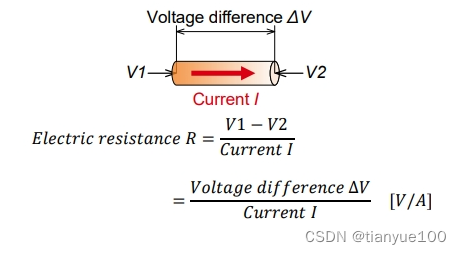
Chart 4 proposes an alternative approach that can be used as a tool for more accurately determining a device’s junction temperature in real‐life application scenarios. This approach eliminates the effect of different heatsinks from the equation. However care must be taken while measuring the case temperature so 1) a non‐contact thermal measurement instrument is recommended and 2) the point of measurement on the case should be as close as possible to the center of its surface.
Conclusion
The results presented above show that determining the junction temperature of a semiconductor device using the various thermal resistance parameters (junction to case, lead or ambient) typically found in a manufacturer’s datasheet are highly dependent on the heatsink arrangement. Instead, chart 4 shows a much closer correlation between junction temperature and case temperature that is far less dependent on the size or effectiveness of any heatsink. Hence a graph similar to chart 4 is the most accurate tool for determining a device’s junction temperature, provided the case temperature can be measured the same way on a real application circuit board.
Basics of Thermal Resistance and Heat Dissipation
Basics of Thermal Resistance and Heat Dissipation (rohm.com)
Challenges in designing electronic equipment include downsizing, improvement in efficiency, support for electromagnetic compatibility (EMC), and countermeasures against heat. Heat has been one of the most important considerations because it affects the performance and reliability of the parts and equipment as well as safety. This application note provides the basics of thermal resistance and heat dissipation considering semiconductor parts such as the ICs and transistors used in electronic equipment.
What is thermal resistance?
Thermal resistance is a quantification of how difficult it is for heat to be conducted. Thermal resistance is represented as the quotient of the temperature difference between two given points by the heat flow between the two points (amount of heat flow per unit time). This means that the higher the thermal resistance, the more difficult it is for heat to be conducted, and vice versa.
R is used as the symbol for the electric resistance, while θ (theta) is used for the thermal resistance. The JEDEC (Joint Electron Device Engineering Council) Solid State Technology Association is a trade organization that standardizes specifications in the field of semiconductor parts. In its integrated circuit thermal measurement method, part of the JESD51 standards, JEDEC has standardized that θXX or RθXX (Theta-XX, if Greek characters are unavailable) should be used. For XX, symbols representing the two given points are entered. For example, θT1T2, RθT1T2, or Theta-T1T2 should be used in the case shown in the figure above.
In addition, the IEC (International Electrotechnical Commission), a global organization that specifies and publishes international standards for all electric, electronic, and related technologies, uses Rth in the EN 60747-15 standards for discrete semiconductor devices.
Based on these relationships, in ROHM’s data sheets, θ is used for ICs, while Rth is used for discrete devices (with some exceptions).
The unit of thermal resistance is K/W or °C/W (K represents kelvins). Although K and °C are different in their absolute values (0 K = -273.15°C), they can be treated equivalently in terms of relative temperatures (K = °C).
Thermal Ohm’s law
The thermal resistance can be considered in the same way as the electric resistance. The basic formulas of thermal calculation can be treated in the same way as Ohm’s law. In the figure below, Ohm’s law is represented with an illustration and equations. It can be seen that the respective parameters are replaceable by heat and electricity.
Therefore, as potential difference ΔV is calculated with R × I, temperature difference ΔT can be calculated with Rth × P.

Heat dissipation path
Generated heat is dissipated to the ambient air via various paths through the conduction, radiation, and convection. In this section, an IC mounted on a printed circuit board (PCB) is used as an example for explanation.
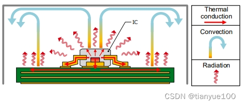
The heat generating source is the chip (die) of the IC. The heat is conducted to the die attach (die bonding), lead frame, case (package), and PCB. The heat is transferred from surfaces of the PCB and the IC package to the atmosphere through the convection and radiation. This is represented with a circuit network of resistance elements as follows.
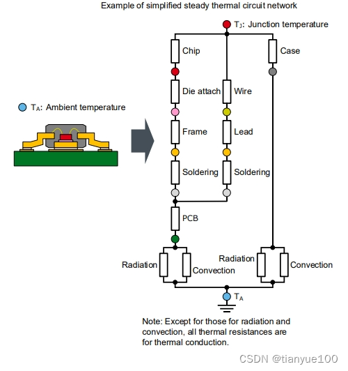
The colors of the respective parts in the IC cross section (the left figure above) correspond to the colors of the circles in the circuit network. For example, the chip is represented in red. Junction temperature TJ of the chip reaches ambient temperature TA through the thermal resistances as shown in the circuit network.
The heat dissipation path runs from the chip to the exposed heat-pad via the die attach and frame, and reaches the PCB via soldering on the copper foil land of the PCB. Then, the heat is transferred to the atmosphere (TA) through the convection and radiation from the PCB.As another possible path, the heat can be transferred from the chip to the lead frame and the PCB via the bonding wire, and convected and radiated to the atmosphere. It is also possible that the heat is convected and radiated from the chip to the atmosphere through the package.
If the thermal resistance of these paths and the power loss of the IC are known, the temperature difference (between TJ and TA in this case) can be calculated with the equation for the thermal resistance as mentioned above.
Thermal design is intended to reduce each thermal resistance described here, that is, to reduce the thermal resistance of the heat dissipation path from the chip to the atmosphere. This reduces TJ and improves reliability.
In the following sections, we explain basic formulas required for reducing each thermal resistance.
Thermal resistance for thermal conduction
Thermal resistance for thermal conduction is represented with the following figure and equations.

The figure shows that temperature T1 at one end of an object with cross section A and length L is transferred to the opposite end through the conduction, changing into temperature T2.
The first equation is the equation for the thermal resistance described in the first section, showing that the temperature difference between T1 and T2 is the product of thermal resistance Rth multiplied by heat flow P.
The second equation represents Rth with the parameters of the object.
As it can easily be imagined from the figure and the terms in the equations, the thermal resistance for thermal conduction can be considered basically in the same way as the sheet resistance of a conductor. The sheet resistance can be calculated with an equation where the thermal conductivity is replaced with the resistivity. As the resistivity has a value specific to the conductor material, the value of thermal conductivity is also specific to the material.
Based on the equation for Rth, in order to reduce the thermal resistance for thermal conduction, it is necessary to increase the cross section of the object, decrease the length of the object, or select a material with a higher thermal conductivity.
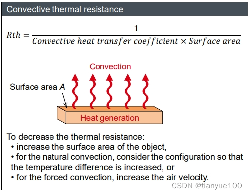
Thermal resistance due to convection (heat transmission)

Thermal resistance due to fluid is represented with the following figure and equations.
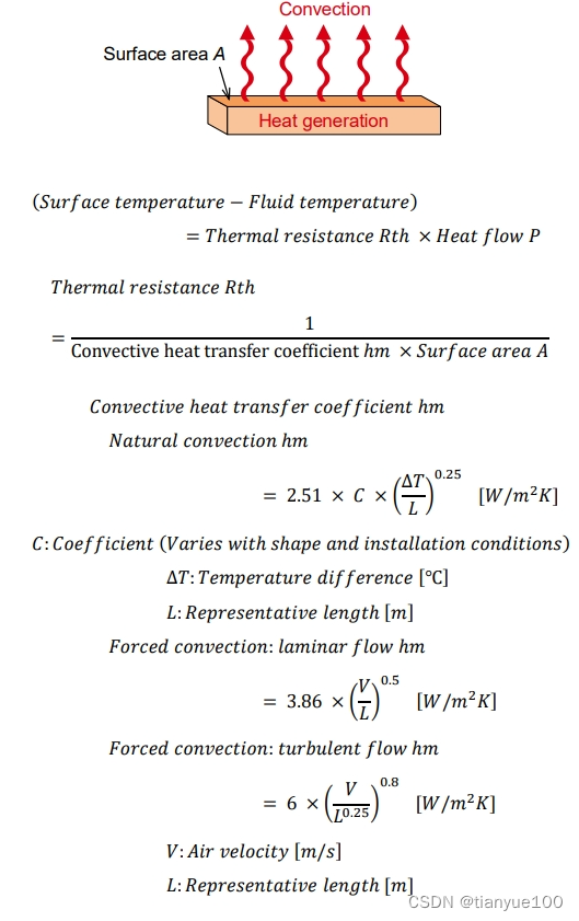
The thermal resistance for convection is represented as the reciprocal of the product of the convective heat transfer coefficient (hm) and the surface area (A) of the object that generates heat. Based on the equation, it is found that the convective thermal resistance is decreased as the surface area of the object is increased.
The convective heat transfer coefficient (hm) depends on the types of convection. For the natural convection, a larger temperature difference facilitates the convection, decreasing the thermal resistance. For the forced convection, it is found that a higher air velocity decreases the thermal resistance.
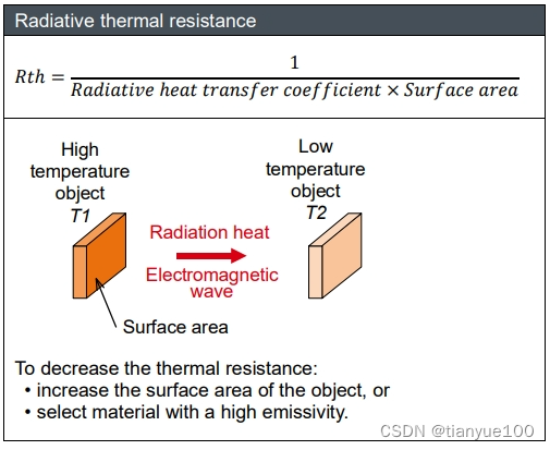
Thermal resistance for heat radiation
The heat radiation occurs by a different mechanism from the thermal conduction or convection (heat transmission) where heat is transferred via molecules. Through the heat radiation, heat can be transferred in a vacuum where no object or fluid exists.
Thermal resistance for heat radiation is represented with the following figure and equations.
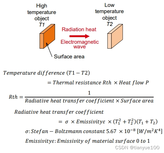
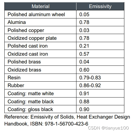
The thermal resistance for heat radiation is represented as the reciprocal of the product of the radiative heat transfer coefficient and the surface area of the object that generates heat. As shown in the equation, the surface area, temperature, and emissivity of the object affects the thermal resistance for heat radiation.
Based on the equation for Rth, in order to reduce the thermal resistance for heat radiation, it is necessary to increase the surface area of the object or select a material with a high emissivity.
For the three forms of heat transfer, namely, thermal conduction, convection (heat transmission), and heat radiation, the equations of the respective thermal resistances have been shown. In all cases, since keys to decrease the thermal resistances can be obtained from the basic formulas, check the relationships of the parameters.
Summary
Finally, we summarize the calculation formulas for the thermal resistances in the three forms of heat transfer and the methods for decreasing the thermal resistances.

Why Thermal Resistance Parameters Are Often Misused
How to Evaluate Junction Temperature Properly with Thermal Metrics (Rev. B)


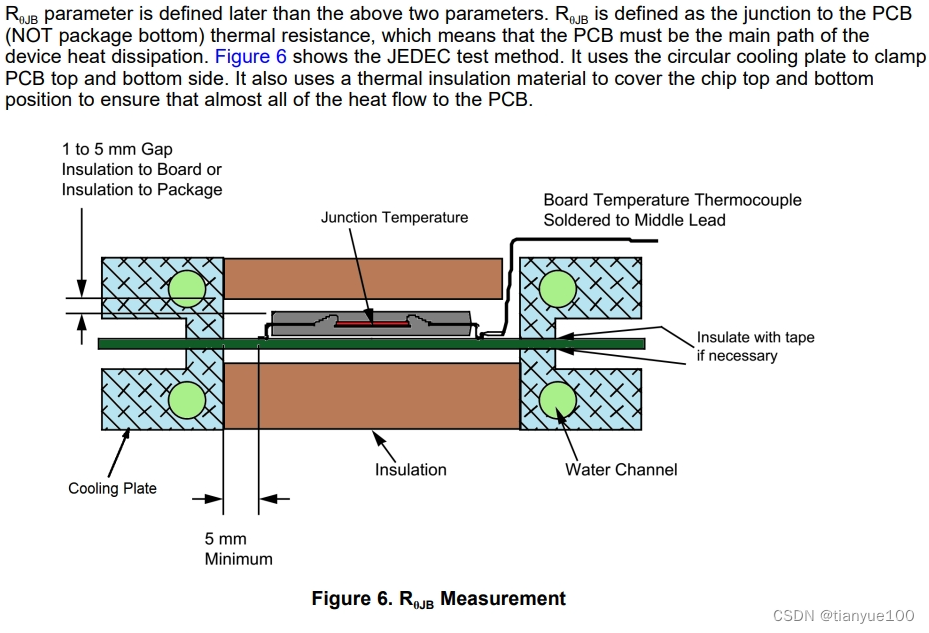

4 About Temperature Measurement
Thermocouple and infrared thermal imager are commonly used for temperature measurement. When a thermocouple measures the temperature, a fine gauge wire (36 to 40 gauge, J or K type wire) must be used to minimize the local cooling from the thermocouple. It must be attached to the center of the package surface (± 1 mm) with a bead of thermally conductive epoxy no larger than 2-mm x 2-mm on a side. Taping the thermocouple to the package surface is not recommended. To minimize the heat sinking impact of the thermocouple, the wire must be dressed along the diagonal of the package, down to the PCB surface, and over a minimum distance of 25 mm before lifting from the PCB. The thermocouple wire can be tacked to the PCB for this routing purpose with tape. Use of improper thermocouple wire gauge can create errors in the measurements of 5-50%.
Temperature measurement with an infrared thermal imager is simple, convenient, fast, and accurate. Depending on the ambient temperature or test environment changes, the machine requires a sufficient preheat stability time before the test. Be sure to correct the reading for the emissivity of the surface being investigated. Choose a high emissivity surface (non-metal, rough, low reflective) on the measured object as a test point. For low emissivity surfaces, apply black insulating tape, spray paint, or apply it with a black water-based stylus pen. Test it vertically at the top of the test point where the test area is well-focused and filled with full display windows.
Regarding air ambient temperature measurement, the PCB must be placed horizontally. Measure the air temp at point 2.54 cm underneath the PCB center and 2.54 cm to the horizontal side. Take the average temperature of two points.
Regarding the PCB temperature testing point, choose the middle position of package side closest to the inside chip. Measure the board temp within 1 mm to the edge of the package, or at the test point recommended by the device vendor. It is best to choose a point where the copper foil is routed and connected to the package. Scratch the solder mask before measurement. For practical operation with a leaded package device, select the center pin on the package long side, measuring temperature at the lead end that is soldered to PCB. If the pin solder pad space to the package edge is larger than 1.5 mm, directly measure the temperature on the board as described above.
Understanding Temperature Specifications: An Introduction
Understanding Temperature Specifications: An Introduction (infineon.com)

Document No. 001-42468 Rev. *I